


The Xn0L is a family of laptop style thin clients fitted with a 15.4" screen. My example is an X90L. I originally purchased an X90LE some time ago that was "...working when put away and not working when I got it back out of the cupboard". My hope that it was just a battery issue was wrong - it was as exactly described: Dead. In December 2011 I bought an X90L, this one one being described as working but the LCD screen had been removed to repair another laptop. It was the work of a few minutes to remove the screenless lid from the new one and replace it by the screen+lid from the old one. Result: One worker.
This X90L was manufactured in May 2009.
Processor Type
SpeedVIA C7-M ULV
1200 MHzChipset VN896 Memory Flash
RAM1GB
1GB (Max 4GB?)Video Screen 15.4" XVGA Widescreen 1280 x 800 Chip
Max resolutionintegrated in CN896
up to ? x ? 32-bit colourPorts Display
Network
USB
Serial
Parallel
PS/21 VGA port 15-pin D-Sub for external monitor (clone mode)
1 DVI-D port for external monitor (clone mode)
10/100/1000
Integrated Wireless 802.11b/g/n
4 x USB2.0
none
none
nonePower Battery
Charger6 cell Li-Ion 4400mAH
19V 3.42A, 5.5mm/2.5mm Coax plugOff
Running0W
~16WDimensions H x W x D (mm) 39.7 x 360 x 260
The operating system is Windows XPe SP2.
For those to whom it matters here is some detail from Linux's /proc/cpuinfo
vendor_id : CentaurHauls cpu family : 6 model : 13 model name : VIA C7-M Processor 1200MHz stepping : 0 flags : fpu vme de pse tsc msr pae mce cx8 apic sep mtrr pge cmov pat clflush acpi mmx fxsr sse sse2 tm nx cpuid pni est tm2 xtpr rng rng_en ace ace_en ace2 ace2_en phe phe_en pmm pmm_en
00:00.0 Host bridge: VIA Technologies, Inc. CN896/VN896/P4M900 Host Bridge
00:00.1 Host bridge: VIA Technologies, Inc. CN896/VN896/P4M900 Host Bridge
00:00.2 Host bridge: VIA Technologies, Inc. CN896/VN896/P4M900 Host Bridge
00:00.3 Host bridge: VIA Technologies, Inc. CN896/VN896/P4M900 Host Bridge
00:00.4 Host bridge: VIA Technologies, Inc. CN896/VN896/P4M900 Host Bridge
00:00.5 PIC: VIA Technologies, Inc. CN896/VN896/P4M900 I/O APIC Interrupt Controller
00:00.6 Host bridge: VIA Technologies, Inc. CN896/VN896/P4M900 Security Device
00:00.7 Host bridge: VIA Technologies, Inc. CN896/VN896/P4M900 Host Bridge
00:01.0 PCI bridge: VIA Technologies, Inc. VT8237/VX700 PCI Bridge
00:02.0 PCI bridge: VIA Technologies, Inc. CN896/VN896/P4M900 PCI to PCI Bridge Controller (rev 80)
00:03.0 PCI bridge: VIA Technologies, Inc. CN896/VN896/P4M900 PCI to PCI Bridge Controller (rev 80)
00:0f.0 IDE interface: VIA Technologies, Inc. VT82C586A/B/VT82C686/A/B/VT823x/A/C PIPC Bus Master IDE (rev 07)
00:10.0 USB Controller: VIA Technologies, Inc. VT82xxxxx UHCI USB 1.1 Controller (rev b0)
00:10.1 USB Controller: VIA Technologies, Inc. VT82xxxxx UHCI USB 1.1 Controller (rev b0)
00:10.2 USB Controller: VIA Technologies, Inc. VT82xxxxx UHCI USB 1.1 Controller (rev b0)
00:10.3 USB Controller: VIA Technologies, Inc. VT82xxxxx UHCI USB 1.1 Controller (rev b0)
00:10.4 USB Controller: VIA Technologies, Inc. USB 2.0 (rev 90)
00:11.0 ISA bridge: VIA Technologies, Inc. VT8237S PCI to ISA Bridge
00:11.7 Host bridge: VIA Technologies, Inc. VT8237/8251 Ultra VLINK Controller
00:13.0 PCI bridge: VIA Technologies, Inc. VT8237A Host Bridge
00:13.1 PCI bridge: VIA Technologies, Inc. VT8237A PCI to PCI Bridge
01:00.0 VGA compatible controller: VIA Technologies, Inc. CN896/VN896/P4M900 [Chrome 9 HC] (rev 01)
02:00.0 Network controller: Ralink corp. RT2860
04:01.0 Audio device: VIA Technologies, Inc. VT8237A/VT8251 HDA Controller (rev 10)
05:06.0 CardBus bridge: Texas Instruments PCIxx12 Cardbus Controller
05:06.2 Mass storage controller: Texas Instruments 5-in-1 Multimedia Card Reader (SD/MMC/MS/MS PRO/xD)
05:06.3 SD Host controller: Texas Instruments PCIxx12 SDA Standard Compliant SD Host Controller
05:06.4 Communication controller: Texas Instruments PCIxx12 GemCore based SmartCard controller
05:07.0 Ethernet controller: Realtek Semiconductor Co., Ltd. RTL-8110SC/8169SC Gigabit Ethernet (rev 10)
The external power supply is rated at 19V 3.42A and is fitted with a 5.5mm/2.5mm coax plug.

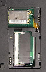
You need to remove the keyboard in order to gain access to some of the memory components. There is also access on the bottom to an additional memory slot and the wireless card.
To remove the keyboard you first need to pop off the panel above the keyboard that carries the on-off switch. There is no need to remove any screws beforehand. It is advisable to disconnect the power and remove the battery before attempting to dismantle the X90L.
You can see a picture of the dismantled X90LE here.
Flash/Disk: The Xn0L has a single 44-pin IDE connector. This is located under the keyboard. Unfortunately there is not much internal space and it would be difficult to fit in anything other than the standard flash module.
Ram: There are two SODIMM sockets to take the RAM. The first is located under the keyboard whilst the second is behind a panel on the bottom of the case. The RAM fitted is made by Apacer and marked 1GB SOD PC2-5300 CL5. I moved the single SODIMM from underneath to the socket under the keyboard. This means I'm left with the easier job of opening the panel on the bottom should I want to add additional memory to the X90L.
SD Card: There is an SD card slot on left hand side just below the Express card slot.
The wireless card is a mini-PCI card which, like the second RAM socket, is located behind a removable panel on the bottom of the case.
The "e" model adds a smart card reader and bluetooth.
In June 2014 I received an email from Simon Fitch. He had been looking to see the optimum amount of memory to install on his x90LW:
"The VIA info for the motherboard suggests it'll take 4GB of RAM. I have installed 2x 2GB of DDR2 667Mhz RAM and indeed it boots up - but the BIOS and Windows only sees 3GB (even with windows having the 3GB and PAE switches enabled for big RAM).
I've used CPUID to look deeper into this, and indeed both modules are recognised as 2GB modules. However it seems that the motherboard and BIOS only sees 1GB on one module - and that isn't due to a 32bit issue. It turns out that the AGP (Graphics) and PCI memory allocations are taking up most of the area above 3GB, so installing 4GB of RAM isn't much help. As the memory is only single banked, there is no speed benefit from installing 2x 2GB modules. The motherboard seems incapable of supporting dual banked mode and, thanks to the AGP/PCI mapping, you would be wasting 1GB RAM anyway. I've therefore installed 1x 2GB under the keyboard and 1x 1GB in the accessible slot for a maximum of 3GB. All seems to be running well so far.
Other interesting info from CPUID is that the motherboard identifies itself as a 'VIA Development Board' and that the graphics is running on a 8x AGP bus rather than a PCI-Express bus which I was expecting!"